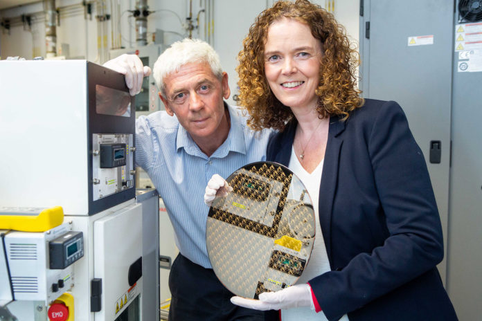
Led by Tyndall National Institute in Ireland, the €4.7 million European Union ASCENT programme provides access to the European nanoelectronics network, and has delivered 100 projects to researchers from 30 countries across the global research community over the last four years.
ASCENT has built a community of over 400 researchers from the nanoelectronics modelling and characterisation research community and has provided free-of-charge access to the unique research infrastructure and expertise in three of Europe’s premier research centres.
ASCENT opened the doors to the world’s most advanced nanoelectronics infrastructures in Europe in May 2015, when leading European nanoelectronics institutes, Tyndall National Institute in Ireland, CEA-Leti in France and imec in Belgium, entered into this collaborative open-access project to mobilise European research capabilities like never before.
Concluding at the end of July 2019, the programme has supported a total of 100 projects from transnational researchers involving customised nanofabrication, a broad range of nano-visualisation and electrical/physical characterisation projects as well as the provision of test wafers, from both imec and CEA-Leti, containing the very latest advanced nano-device technologies.
During the course of the programme, ASCENT shared the best scientific and technological practices, formed a knowledge-innovation hub, trained new researchers in advanced methodologies and established a unique research network of advanced technology designers, modellers and manufacturers in Europe. All this helped to strengthen Europe’s knowledge in the integral area of nanoelectronics research.
Julie Donnelly, Programme Manager, Tyndall National Institute said: “The three partners each provided researchers with a unique opportunity to access advanced device data, test chips, fabrication facilities and characterisation equipment at Tyndall, imec and CEA-Leti. This enabled the research community to explore exciting new developments in industry and meet the challenges created in an ever-evolving and demanding digital world.
“During the programme, we undertook an extensive promotion campaign including a series of workshops and a dedicated accelerator programme for PhD students in order to reach as many researchers as possible. The feedback from the users was always very positive and they valued the opportunity to have rapid free-of-charge access to our facilities and collaborate with our experts.”
The partners’ respective facilities are truly world-class, representing over €2 billion of combined research infrastructure with unique credentials in advanced semiconductor processing, nanofabrication, heterogeneous and 3D integration, electrical characterisation and atomistic and TCAD modelling.
This is the first time that access to these state-of-the-art devices and test structures became available anywhere in the world.
The project engages industry directly through an ‘Industry Innovation Committee’ and fed back the results of the open research to device manufacturers, giving them crucial information to improve the next generation of electronic devices.
This project received funding from the European Union’s Horizon 2020 research and innovation programme under Grant Agreement No. 654384.


